Follow 


Engineered for extreme thermal stability, chemical inertness, and ultra-fine dispersion across semiconductor processing and industrial manufacturing.
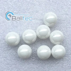
As semiconductor fabrication transitions below 3nm nodes and wide-bandgap (WBG) power electronics surge, the demand for high-k dielectric gate oxides, ultra-pure ceramic gate rings, and sub-nanometer polishing media has reached unprecedented thresholds.
In modern microelectronics, the transistor gate serves as the central control electrode governing electron flow between source and drain terminals. Whether implemented in sub-nanometer planar MOSFETs, 3D FinFETs, Gate-All-Around (GAA) RibbonFET architectures, or high-power Gallium Nitride (GaN) and Silicon Carbide (SiC) power devices, gate integrity directly determines switching velocity, gate leakage density, breakdown voltage, and dynamic energy efficiency.
As a premier High-Quality Transistor Gate Supplier & Exporters, Pingxiang Baitian (Ball-tec) New Materials Co., Ltd. integrates decades of advanced ceramic synthesis, nanometer-level powder processing, and precision sintering technology to deliver high-performance ceramic materials engineered specifically for semiconductor gate processing environments and power transistor thermal isolation.
Traditional silicon dioxide (SiO2) gate dielectrics suffer from severe quantum mechanical tunneling leakage at film thicknesses under 1.2nm. Advanced transistor gate engineering relies on high-k dielectric materials—primarily Hafnium Oxide (HfO2), Yttria-Stabilized Zirconia (YSZ), and Ultra-High Purity Alumina (Al2O3)—to maintain electrostatic gate control while physically increasing barrier thickness. Our advanced ceramic substrates and ultra-fine polishing media provide the baseline purity required to manufacture defect-free gate structures across advanced foundry nodes.
Ultra-low alkali ion concentration (<5ppm Na/K) prevents mobile charge contamination across delicate gate dielectric stack structures during CVD/ALD deposition processes.
Engineered Yttria-stabilized zirconia and high-density alumina ceramic components withstand aggressive fluorinated and chlorinated plasma etch regimes in gate-patterning chambers.
Our ultra-fine ZrO2 and Al2O3 micro-grinding media facilitate CMP slurries achieving surface roughness Ra < 0.15nm, minimizing gate oxide thickness variation.
Comparative physical, thermal, and electrical metrics of advanced ceramic formulations utilized in gate dielectric synthesis, etch rings, wafer chucks, and chemical-mechanical planarization (CMP).
| Material Formulation | Purity Grade | Dielectric Constant (k) | Breakdown Voltage (kV/mm) | Thermal Conductivity (W/m·K) | Key Transistor Gate Application |
|---|---|---|---|---|---|
| Yttria-Stabilized Zirconia (3Y-TZP) | 99.95% | 25 - 30 | 15 - 20 | 2.5 - 3.0 | High-k gate dielectrics, micro-polishing media for CMP, high-toughness isolation rings |
| Ultra-High Purity Alumina (Al2O3) | 99.999% (5N) | 9.8 | 20 - 25 | 30 - 35 | Gate insulator layers in GaN HEMT, plasma etch chamber gate rings, electrostatic chucks |
| Silicon Nitride (Si3N4) | High-Density Sintered | 7.5 | 18 - 22 | 85 - 90 | Passivation layers for high-power transistor gates, robotic transfer end-effectors, high-speed bearings |
| Zirconia-Toughened Alumina (ZTA) | Composite Matrix | 12 - 14 | 16 - 19 | 24 - 28 | Heavy-duty chemical milling, structural gate-processing fixtures, wear-resistant guide components |
From front-end-of-line (FEOL) gate oxide deposition to back-end packaging of high-frequency power transistors, our ceramic solutions meet rigid process windows.
In sub-3nm gate-all-around nano-sheet architectures, atomic layer deposition (ALD) of gate oxide stacks demands precursor media and milling balls of pristine purity. Trace metallic impurities (such as Fe, Ni, or Cr) cause mid-gap state traps, leading to threshold voltage fluctuations. Baitian's 99.999% alumina and high-density YSZ micro-beads deliver zero-contamination wet milling for ALD target powder preparation, ensuring stable transistor switching thresholds across billions of logic gates per die.
Gallium Nitride High Electron Mobility Transistors (GaN HEMTs) and Silicon Carbide Power MOSFETs operate at junction temperatures exceeding 200°C and electric field intensities above 3 MV/cm. The ceramic gate insulator stack must exhibit high thermal conductivity, exceptional dielectric breakdown resistance, and low thermal expansion mismatch with WBG substrates. Our engineered alumina ceramic insulators and precise silicon nitride components provide structural protection and heat dissipation for automotive inverter power gates and 5G RF power amplifiers.
During dry plasma etching of metal gate electrodes (such as TiN, TaN, or W gate stacks), reactive chlorine and fluorine ions rapidly degrade standard chamber components. Degradation releases macro-particles that land on wafers, causing gate-short defects. Baitian’s high-purity sintered zirconia and alumina ceramic etch rings retain surface microstructural integrity under intense RF plasma bias, drastically extending chamber maintenance cycles and maximizing wafer yield.
Combining rare-earth raw material reserves, fully integrated industrial supply chains, and state-of-the-art sintering infrastructure in Pingxiang, Jiangxi.
China commands over 70% of global rare-earth refining capacity. Direct access to high-purity Yttrium, Zirconium, and Aluminum precursors ensures cost stability and continuous supply security for worldwide semiconductor customers.
Located in the heart of Pingxiang's Ceramic Industrial Park, our 100,000m² facility controls the complete manufacturing chain—from spray drying, cold isostatic pressing (CIP), to high-temperature gas-pressure sintering (GPS).
Through high-volume automated production and optimized thermal energy cycles, Baitian delivers SEMI-compliant precision components at 30% to 50% lower total cost of ownership compared to European or Japanese counterparts.
How semiconductor fab procurement managers and OEM component buyers validate suppliers against global quality standards.
Sourcing precision ceramic components for transistor gate processing requires comprehensive qualification processes. International buyers evaluate suppliers based on rigid technical criteria, batch-to-batch consistency, cleanroom packaging standards, and supply chain transparency.
Analyzing the convergence of AI chip scaling, high-frequency mobility, and next-generation power conversion.
AI accelerators and GPU clusters require aggressive reduction in parasitic gate capacitance. Advanced ceramic insulators enable higher switching frequencies without thermal runaway in AI data center servers.
800V EV architectures demand SiC/GaN power transistor gates operating under harsh thermal cycle stresses. High-toughness YSZ ceramics provide dynamic electrical isolation preventing gate dielectric arc failures.
As Moore's Law slows down, heterogeneous chiplet integration relies on ultra-flat ceramic carrier substrates and precision polishing media to ensure nanometer-scale interposer gate alignment.
Expert responses from our senior materials research team addressing common engineering, procurement, and application queries.
Explore our full line of industrial catalyst support spheres, high-density grinding beads, and gas dehydration adsorbents.