Follow 


Explore our premium selection of advanced zirconia, high-purity alumina grinding media, and molecular sieves engineered to empower modern electronic board production, micro-milling, and chemical gas purification.
As power densities escalate in electric mobility, 5G/6G wireless infrastructure, and high-frequency aerospace avionics, standard organic FR-4 and metallic core circuit substrates hit severe thermal and electrical limits. Modern electronic boards rely heavily on advanced ceramic substrates—primarily Alumina ($\text{Al}_2\text{O}_3$), Zirconia-Toughened Alumina (ZTA), and Silicon Nitride ($\text{Si}_3\text{N}_4$).
Traditional organic electronic printed circuit boards (PCBs) possess low thermal conductivity ($\sim 0.25 \text{ W/m}\cdot\text{K}$), causing rapid heat accumulation, thermal expansion mismatch, and component degradation in high-power modules. In contrast, ceramic electronic boards deliver thermal conductivity up to $170-200 \text{ W/m}\cdot\text{K}$ while retaining high dielectric breakdown strength ($>20 \text{ kV/mm}$).
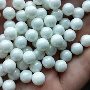
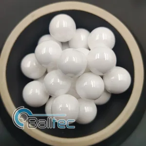
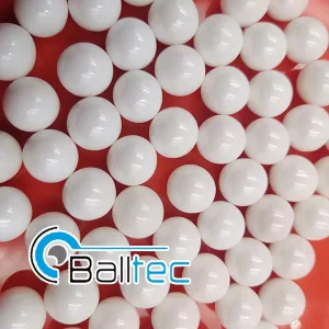
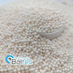
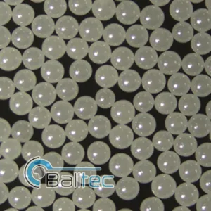
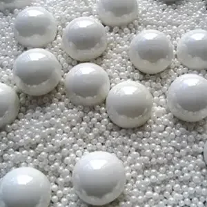
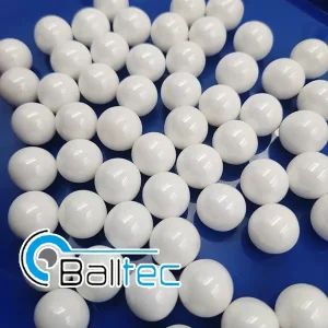
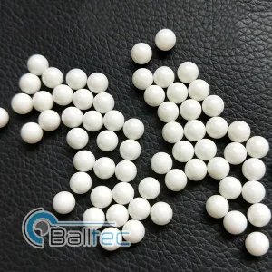
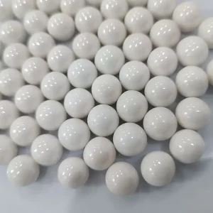
To manufacture these flawless ceramic substrates, ultra-fine raw ceramic powders must undergo sub-micron dispersion milling. Utilizing low-wear, high-density Yttria-Stabilized Zirconia (YSZ) grinding beads guarantees zero metallic contamination during powder preparation, directly preserving the insulation resistance and breakdown voltage of final circuit boards.
China has established an integrated ecosystem encompassing upstream ceramic mineral processing, chemical synthesis of ultra-pure zirconia and alumina powders, tape casting, metallization (DBC, DPC, AMB), and final SMT assembly. Sourcing electronic board materials and substrates directly from verified Chinese manufacturers unlocks massive economies of scale, strict batch-to-batch repeatability, and customized substrate geometries.
| Substrate Material Type | Thermal Conductivity ($\text{W/m}\cdot\text{K}$) | CTE Matching ($\text{ppm/K}$) | Dielectric Constant (@1MHz) | Bending Strength ($\text{MPa}$) | Primary Electronic Board Application |
|---|---|---|---|---|---|
| FR-4 High TG | 0.3 - 0.5 | 14.0 - 17.0 | 4.5 | 350 | Standard Consumer Electronics, Low-Power Controllers |
| Direct Bond Copper (DBC) $\text{Al}_2\text{O}_3$ | 24 - 35 | 6.8 - 7.2 | 9.8 | 400 | Industrial Motor Drives, Solar Inverters, Power Supplies |
| Direct Plated Copper (DPC) ZTA | 35 - 50 | 5.5 - 6.2 | 10.2 | 700 | High-Power LED Matrices, Automotive Headlamps |
| Active Metal Brazed (AMB) $\text{Si}_3\text{N}_4$ | 80 - 90 | 2.5 - 3.0 | 8.3 | 850+ | EV SiC Main Inverters, Wind Turbine Power Modules |
Achieving optimal signal integrity and high-current carry capacity in modern electronic boards requires synergistic advancement across ceramic powder synthesis, substrate planarization, and surface metallization pathways.
Utilizes a high-temperature eutectic melting process ($\approx 1065^\circ\text{C}$) to bond thick oxygen-containing copper foils directly to alumina ceramic boards. Ideal for high-voltage industrial power modules requiring robust current routing.
Combines thin-film vacuum sputtering with photolithography and electroplating to deposit ultra-precise copper traces (line width/spacing down to $20\,\mu\text{m}$) on ultra-flat ceramic substrates. Essential for high-density RF circuits and optoelectronics.
Uses active element braze alloys (Ti, Zr) under high vacuum to join heavy copper layers onto Silicon Nitride ($\text{Si}_3\text{N}_4$) or Zirconia substrates. Represents the pinnacle of thermal shock resilience for EV traction inverters.
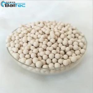
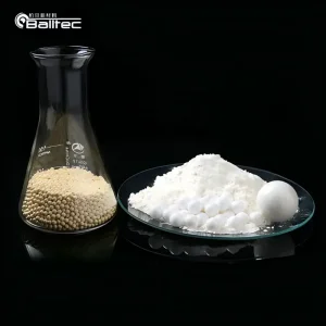
During the tape-casting phase of ceramic electronic board production, slurries containing $\text{Al}_2\text{O}_3$ or $\text{ZrO}_2$ must be milled to strict particle size distribution ($D_{50} < 0.4\,\mu\text{m}$). The use of premium China-manufactured Low-Impurity Zirconia Grinding Media prevents pinholes, voids, and micro-cracks during high-temperature sintering ($1550^\circ\text{C}-1700^\circ\text{C}$). Furthermore, atmosphere control furnaces utilize specialized 13X and 4A Molecular Sieves to eliminate trace moisture and gaseous contaminants, guaranteeing defect-free ceramic dielectric properties.
Leveraging Pingxiang’s industrial ceramic cluster alongside southern China’s electronics manufacturing ecosystem provides unmatched agility, supply chain security, and cost efficiency for international procurement partners.
Direct integration with domestic zircon sand purification plants and calcined alumina refineries isolates global buyers from international geopolitical supply shocks, ensuring steady pricing and uninterrupted production runs.
Equipped with state-of-the-art Japanese laser scribing tools, high-speed multi-spindle CNC drilling units, and continuous tunnel kilns, achieving strict surface flatness ($< 0.02\text{ mm}$) and warpage tolerances.
Robust export packaging compliance (UN-certified sea/air freight containers, moisture-barrier vacuum sealing) ensures zero oxidation or mechanical damage during international shipping to Europe, North America, and SEA.
Ceramic electronic boards engineered in China are now operating at the core of critical mission-critical applications across global technology hubs.
Silicon Carbide (SiC) MOSFET power devices operate at junction temperatures exceeding $175^\circ\text{C}$ with high switching frequencies. AMB Silicon Nitride and DBC ZTA ceramic electronic boards provide extreme flexural strength and Coefficient of Thermal Expansion (CTE) matching closely with SiC dies, preventing thermal fatigue and substrate delamination in vehicle power units.
At millimeter-wave (mmWave) frequencies, transmission line loss and dielectric dissipation must be minimized. DPC ceramic electronic boards fabricated with 99.6% Alumina substrates deliver exceptionally low dielectric loss ($\tan \delta < 0.0004$), serving as ideal circuit platforms for active antenna units (AAU) and power amplifiers.
Concentrated LED arrays used in industrial UV curing, medical sterilization, and automotive matrix illumination generate localized heat fluxes exceeding $100 \text{ W/cm}^2$. Ceramic electronic boards rapidly pull heat away from LED junctions, doubling operating lifetimes and maintaining optical output lumen stability.
Exposed to severe mechanical shock, continuous vibration, and ambient temperatures up to $300^\circ\text{C}$, standard PCBs fail instantly. Ceramic electronic boards maintain structural rigidity and hermetic electrical isolation under hostile downhole oil field conditions and space-bound environments.
Operating under ISO 9001:2015, ISO 14001, and ISO 45001 management frameworks, our products adhere strictly to international environmental and safety directives.
Fully compliant with EU RoHS Directive 2011/65/EU and REACH (EC 1907/2006) regulations. Free from toxic heavy metals, lead, halogenated flame retardants, or SVHC substances.
Every ceramic electronic board substrate lot undergoes 100% C-SAM (Scanning Acoustic Microscopy) void detection, X-Ray fluorescence (XRF) copper thickness verification, and laser profilometer surface roughness measurement.
Our dedicated R&D engineering unit offers DFM (Design for Manufacturability) guidance, substrate thermal simulation, prototype fast-turn turnaround (in as fast as 5 business days), and custom panelization.
Technical answers for procurement officers, process engineers, and supply chain managers evaluating Chinese ceramic electronic board suppliers.
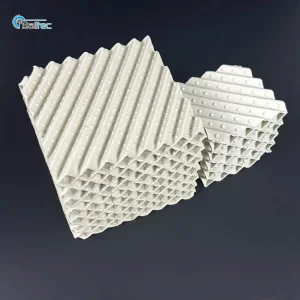
Explore our full export series including high-purity zirconia grinding beads, tower packing structures, bearing balls, and specialized powders built for demanding global manufacturing plants.