Follow 


Essential ultra-pure ceramic substrates, grinding media for fine drill conditioning, and structural components tailored for next-generation printed circuit board (PCB) and electronic assembly lines.
The global electronic printed circuit board (PCB) sector is undergoing a monumental technological paradigm shift. Driven by the aggressive proliferation of 5G/6G telecommunication networks, Artificial Intelligence (AI) hyperscale data centers, Electric Vehicle (EV) powertrains, and autonomous aerospace navigation, enterprise buyers no longer evaluate PCB manufacturers solely on unit price. Modern procurement demands comprehensive thermal management capability, signal integrity at millimeter-wave frequencies, extreme mechanical robustness, and zero-defect quality controls.
As silicon and wide-bandgap (SiC and GaN) semiconductor chips shrink while power densities surge beyond historical limits, conventional FR-4 and polyimide substrates face severe operational bottlenecks. High power dissipation leads to thermal stress, dielectric breakdown, signal attenuation, and structural warping. To address these systemic hurdles, leading PCB suppliers integrate advanced material engineering—specifically Alumina (Al₂O₃), Zirconia (ZrO₂), ZTA (Zirconia Toughened Alumina), and Silicon Nitride (Si₃N₄) ceramic substrates—alongside state-of-the-art micro-drilling milling equipment serviced by ultra-precise grinding media.
To assist procurement officers, thermal engineers, and system architects in selecting optimal substrate configurations, our research team has mapped out the electro-thermal and mechanical parameters comparing traditional PCB laminates against ceramic-reinforced interconnect systems:
| Substrate Material Class | Thermal Conductivity (W/m·K) | CTE Matching (ppm/K) | Dielectric Constant (Dk @ 1GHz) | Flexural Strength (MPa) | Primary Industrial Use-Cases |
|---|---|---|---|---|---|
| Standard FR-4 Glass-Epoxy | 0.25 - 0.40 | 14 - 17 (Poor) | 4.4 - 4.8 | 350 | General Consumer Electronics, IoT Nodes |
| High-Tg Polyimide (Rigid-Flex) | 0.30 - 0.50 | 12 - 16 | 3.2 - 3.6 | 220 | Aerospace Avionics, Wearable Modules |
| 96% Alumina Ceramic (Al₂O₃) | 24 - 28 | 6.8 (Close to Silicon) | 9.6 | 400 | LED Arrays, Automotive Sensors, DBC Circuits |
| Zirconia Toughened Alumina (ZTA) | 28 - 35 | 7.2 | 9.8 | 700 - 850 | High-Vibration Automotive Power Inverters |
| Silicon Nitride (Si₃N₄ AMB) | 80 - 90 | 3.0 (Ideal for SiC) | 8.3 | 900 - 1100 | 800V EV Traction Inverters, Military Radar |
Utilizes high-temperature eutectic melting process to bond heavy copper foils (140µm–500µm) directly onto Al₂O₃ or AlN ceramic plates. Delivers exceptional current carrying capacity and rapid heat spreading for industrial motor drives.
Employs active titanium/silver brazing alloys to fuse thick copper layers onto Silicon Nitride (Si₃N₄). Offers maximum thermal fatigue resistance under intense dynamic power cycling (-55°C to +175°C).
Combines thin-film vacuum sputtering and micro-electroplating for ultra-fine trace pitch (<50µm). Ideal for high-density laser diodes, optical transceivers, and micro-scale RF packages.
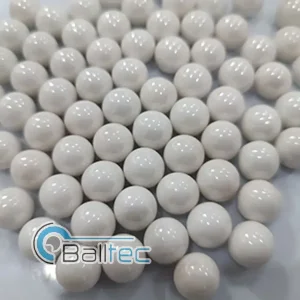
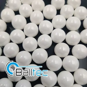
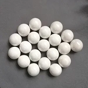
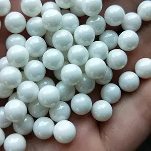
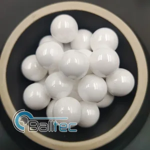
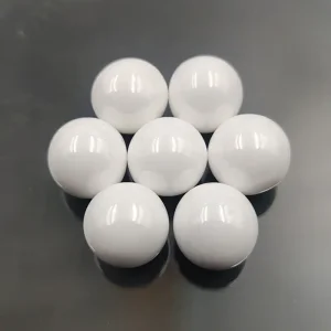
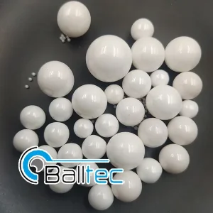
High-aspect-ratio micro-vias in multilayer PCBs demand extreme spindle speeds. Precision ceramic bearing balls and YSZ grinding media guarantee ultra-fine drill bit sharpness and polished surface finishes.
As a trusted global supplier and manufacturer, we engineer full-stack circuit board and raw material solutions tailored to the operational stresses of specific industrial sectors:
EV 800V architecture requires circuit boards capable of handling high voltage spikes and immense thermal dissipation. Our Si₃N₄ AMB and ZTA ceramic substrate PCBs prevent dielectric breakdown while providing 10x longer power-cycle life compared to conventional insulated metal substrates (IMS).
High-frequency computing demand signal propagation without phase distortion. Utilizing low-loss ceramic fillers, high-purity alumina backplanes, and smooth copper foil profiles, our high-speed PCBs minimize Insertion Loss and Crosstalk up to 77 GHz RF bands.
Mission-critical avionics demand zero component failure under severe mechanical vibration and radiation shocks. Our IPC Class 3 rigid-flex ceramic interconnects maintain structural integrity across outer-space vacuum and cryogenic temperatures.
The evolution of electronic circuit boards over the next decade will be defined by continuous miniaturization, embedded active/passive components, and green zero-emission manufacturing. The roadmap below outlines the key technological milestones driven by our joint R&D laboratories:
Transitioning from subtractive etching to multi-material additive manufacturing. Direct ink writing (DIW) of conductive silver/copper nanoparticles onto 3D-structured ceramic bodies eliminates hazardous chemical waste while allowing non-planar circuit routing.
Integrating micro-channel liquid cooling passages directly inside multilayer ceramic substrate PCBs (LTCC/HTCC). This enables direct-die contact cooling, solving heat fluxes exceeding 500 W/cm² in AI accelerator chips.
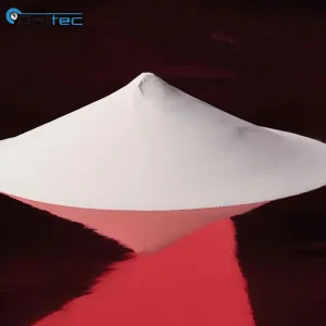
As micro-via diameters drop below 50 micrometers, drilling pastes and chemical mechanical planarization (CMP) slurries require sub-micron Yttria-stabilized zirconia media for flawless surface planarity without micro-cracks.
As a globally recognized manufacturer and exporter headquartered in the Pingxiang Ceramic Industrial Park, Jiangxi, China, our 100,000 m² integrated production campus operates under stringent international quality control systems. Founded by technical experts with decades of research background in Japanese and American advanced ceramic labs, we guarantee full supply chain traceability from raw powder preparation to final electrical probing.
Fully compliant with ISO 9001:2015, ISO 14001:2015, and ISO 45001:2018 management systems. Automotive product lines conform to strict IATF 16949 production part approval processes (PPAP Level 3).
All materials comply with EU RoHS 3.0 (Directive 2015/863) and REACH regulations. Halogen-free laminates and lead-free surface finishes (ENIG, ENEPIG, Immersion Silver) ensure compliance with global eco-design mandates.
100% Flying Probe Testing, Automated Optical Inspection (AOI), X-Ray Fluorescence (XRF) coating thickness verification, Thermal Shock Cycling (-65°C to +150°C), and Ionic Contamination Testing.
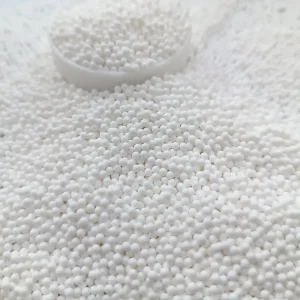
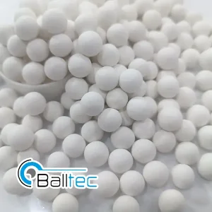
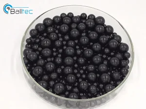
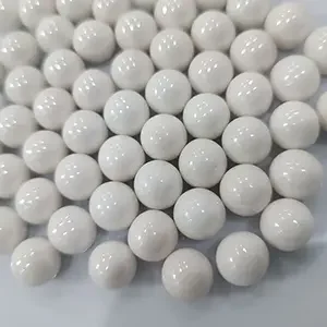
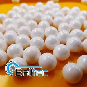
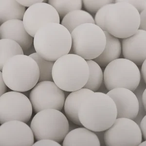
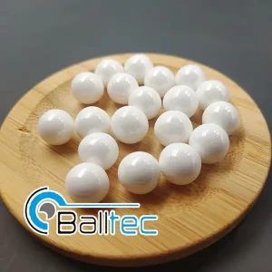
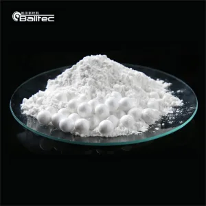
Discover our comprehensive lineup of wear-resistant zirconia beads, high-purity alumina grinding media, precision bearing balls, and high-purity oxides engineered for modern electronic manufacturing lines.