Follow 


Explore our factory-direct ceramic media, chemical processing packing, ultra-pure components, and micro-engineered materials powering global IC manufacturing lines.
The global Integrated Circuit (IC) industry is undergoing a structural transformation driven by artificial intelligence (AI), sub-3nm nanometer lithography scaling, autonomous mobility, and high-performance computing (HPC). As microchip architecture migrates toward 3D Gate-All-Around (GAAFET) and Complementary FET (CFET) designs, semiconductor fabrication plants (fabs) face unprecedented physical and mechanical challenges. Yield optimization no longer depends strictly on optical photolithography; it hinges heavily on the chemical purity, ultra-precise mechanical polishing, and thermal stability of auxiliary process materials.
Leading global IC suppliers and semiconductor foundries require raw material ecosystems engineered to sub-nanometer specifications. From Chemical Mechanical Planarization (CMP) slurries that rely on ultra-high purity 99.999% alumina ($Al_2O_3$) and yttria-stabilized zirconia ($ZrO_2$) nanoparticles to vacuum-compatible silicon nitride ($Si_3N_4$) ceramic bearings for extreme cleanroom robotics, every sub-component directly dictates fab throughput, defect density, and mean-time-between-failures (MTBF).
Empowering front-end wafer processing, chemical purification, and ultra-precision packaging with state-of-the-art materials engineering.
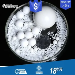
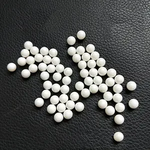
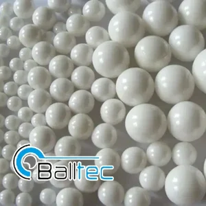
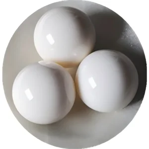
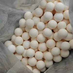
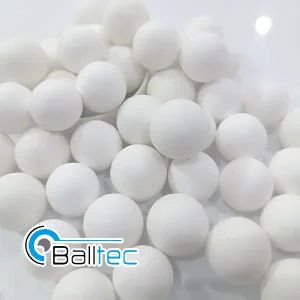
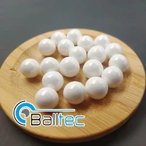
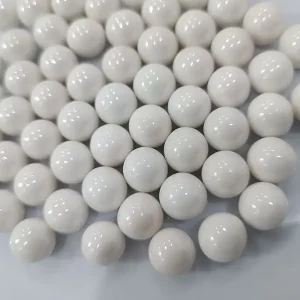
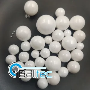
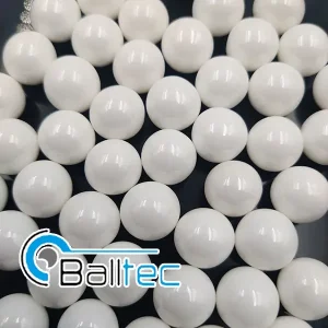
Precision-engineered yttria-stabilized zirconia ($ZrO_2$) and high-purity alumina ($Al_2O_3$) beads enable uniform sub-micron dispersion in chemical mechanical planarization slurries, eliminating micro-scratches on copper interconnects and dielectric layers.
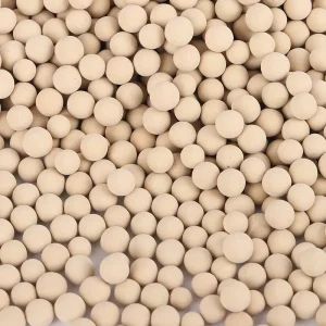
Zeolite 4A, 5A, and 13X molecular sieves remove micro-traces of moisture ($H_2O$), hydrocarbons, ammonia ($NH_3$), and methanol ($CH_3OH$) from specialty gas streams, ensuring pure chemical delivery for atomic layer deposition (ALD).
Grade G3 and G5 silicon nitride ($Si_3N_4$) and zirconia bearing balls offer zero electromagnetic interference, extreme friction reduction, and zero outgassing in vacuum wafer handlers and EUV lithography tracks.
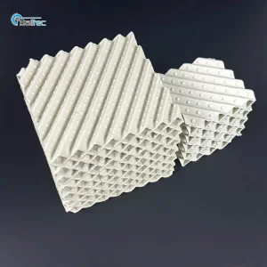
Ceramic corrugated structured packing and Raschig/Pall rings provide anti-corrosive chemical stripping and distillation support for semiconductor wet chemical synthesis plants, reducing energy consumption and boosting yield.
Selecting appropriate materials for IC processing requires rigorous technical validation. The following matrix outlines key physical, thermal, and chemical performance indicators across our primary product line for fab purchasing managers and process engineers.
| Material Classification | Primary Composition | Density / Porosity | Vickers Hardness (HV) | Key IC Fab Application |
|---|---|---|---|---|
| Yttria-Stabilized Zirconia (YSZ) | $95\% ZrO_2 + 5\% Y_2O_3$ | $\ge 6.0 \text{ g/cm}^3$ | $1250 \text{ HV}_{10}$ | CMP Nanoparticle Milling Sub-micron CMP Slurry dispersion |
| High-Purity Alumina (4N Grade) | $\ge 99.99\% Al_2O_3$ | $\ge 3.92 \text{ g/cm}^3$ | $1600 \text{ HV}_{10}$ | Zero-Contamination Ball Milling Wafer polishing substrate, battery materials |
| Silicon Nitride ($Si_3N_4$) Spheres | $\ge 93\% Si_3N_4$ | $3.25 \text{ g/cm}^3$ | $1700 \text{ HV}_{10}$ | Cleanroom Bearings G3 Precision robotics, high-speed spindles |
| Zeolite 4A / 13X Molecular Sieves | Aluminosilicate Framework | Pore diameter $4\text{\AA} - 10\text{\AA}$ | High Crush Strength | Gas Purification Dew point control down to $-70^\circ\text{C}$ in cleanrooms |
| Ceramic Corrugated Packing | Acid-Proof Silicate Matrix | Bulk Density $0.55-0.75 \text{ g/cm}^3$ | Thermal Shock Resistant | Acid Stripping Distillation columns for ultrapure wet chemicals |
Ensuring supply chain continuity, zero line-stoppage, and adherence to international environmental regulations.
Operating a semiconductor integrated circuit factory requires non-negotiable supply continuity. Our manufacturing headquarters in the Pingxiang Ceramic Industrial Park integrates raw powder synthesis, isopressing, high-temperature tunnel kiln sintering, and micro-polishing under an ISO 9001:2015 Quality Management System, ISO 14001 Environmental Standard, and ISO 45001 Occupational Health Assurance.
To eliminate lead time volatility for global IC suppliers, we maintain strategically positioned regional distribution hubs across East Asia, Europe, and North America. Every shipment includes comprehensive documentation: Batch-specific Technical Data Sheets (TDS), X-ray Fluorescence (XRF) purity analysis, scanning electron microscopy (SEM) grain distribution graphs, Certificate of Analysis (CoA), and RoHS/REACH compliance certificates.
Our material solutions cater to distinct specialized sectors within the broader integrated circuit and electronics ecosystem:
Automotive microcontrollers and power management ICs (PMICs) demand zero material defects. Our high-purity alumina grinding media ensures ultra-fine grain size control during the synthesis of substrate ceramics and lead-frame coatings.
Advanced 2.5D/3D chiplet packaging (such as CoWoS) requires CMP slurries with narrow size distributions to flatten interposers without dishing or erosion. Our YSZ zirconia micro-beads deliver precise particle refinement down to sub-50 nanometer scales.
Semiconductor gas suppliers use our 4A and 13X molecular sieves in high-pressure pressure-swing adsorption (PSA) towers to purify carrier gases (Nitrogen, Argon, Helium) to 99.9999% purity levels prior to cleanroom injection.
As the semiconductor industry advances toward sub-1nm logic nodes and quantum computing architectures, conventional process materials reach physical limits. Our ongoing engineering roadmap centers on three breakthrough vectors:
Developing next-generation spherical zirconia particles with a polydispersity index (PDI) below 0.02, allowing ultra-smooth CMP polishing for EUV mask blanks and next-gen oxide chemical planarization.
Integrating hydrogen-fired electric tunnel kilns to achieve carbon-neutral production for high-purity ceramic balls and packing materials, directly supporting major semiconductor foundries in achieving Scope 1 and Scope 2 net-zero sustainability goals.
Pioneering composite silicon nitride and aluminum nitride ($AlN$) structural parts for high-heat dissipation environments inside plasma etching chambers and high-temperature ion implantation systems.
Clear technical insights regarding selection, performance metrics, qualification, and lead times.
Factory-direct sourcing options for ball milling, surface refinement, gas drying, and tower mass transfer.