Follow 


Direct factory supply of precision dielectric media, molecular sieves, and micro-milling ceramics optimized for semiconductor manufacturing and component formulation.
An authoritative analysis on material engineering, gate dielectric capacitance, sub-micron powder synthesis, and high-frequency power electronics infrastructure.
In the contemporary semiconductor and high-voltage power management landscape, Metal-Oxide-Semiconductor Field-Effect Transistors (MOSFETs) and Multilayer Ceramic Capacitors (MLCCs) represent the foundational building blocks of modern electronic infrastructure. As industrial electrification accelerates—driven by Electric Vehicle (EV) powertrains, renewable energy solar/wind inverters, 5G/6G telecommunications infrastructure, and AI-driven data center power delivery systems—the commercial demand for wholesale MOSFET capacitors and high-k dielectric materials has reached an unprecedented zenith.
The global MOSFET and high-frequency capacitor industry is currently undergoing a transformative technological shift. Legacy silicon-based planar MOSFETs are rapidly yielding market share to Wide-Bandgap (WBG) semiconductors, notably Silicon Carbide (SiC) and Gallium Nitride (GaN) devices. These next-generation power transistors operate at exponentially higher switching frequencies ($>1\text{ MHz}$), elevated thermal thresholds ($>200^\circ\text{C}$), and intense electric field breakdowns. Consequently, the capacitive components integrated into gate drivers, snubber circuits, and DC-link filtering networks must exhibit ultra-low Equivalent Series Resistance (ESR), minimal Equivalent Series Inductance (ESL), and superb dielectric thermal stability.
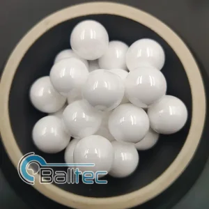
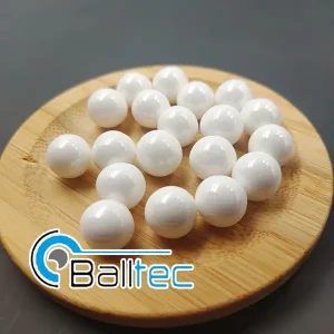
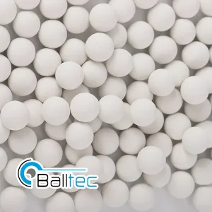
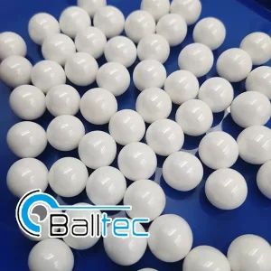
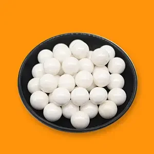
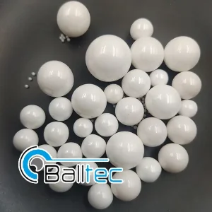
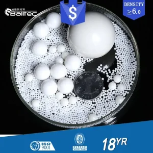
Key Market Takeaway: Modern power MOSFET topologies rely heavily on high-purity ceramic dielectric materials (such as $TiO_2$, $BaTiO_3$, and Yttria-Stabilized Zirconia $ZrO_2$). Achieving zero-defect dielectric layers requires sub-micron ultra-fine powder refining—a domain where advanced zirconia grinding media and high-purity alumina spheres play a decisive role.
At the fundamental device physics level, the performance of a MOSFET is governed by its parasitic capacitance parameters: Gate-to-Source capacitance ($C_{gs}$), Gate-to-Drain reverse transfer capacitance ($C_{gd}$ or $C_{rss}$), and Drain-to-Source output capacitance ($C_{ds}$). Controlling gate-oxide integrity requires extreme precision during the deposition of ultra-thin insulating dielectrics. When manufacturing discrete ceramic capacitors paired with MOSFET gate drivers, raw material purity directly dictates breakdown voltage ($V_{BR}$) and temperature coefficient stability (X7R, X8R, and C0G/NP0 characteristics).
High-power MOSFET circuits operating under high $\frac{dV}{dt}$ and $\frac{dI}{dt}$ switching transients require capacitors with sub-milliohm ESR. Ultra-dense ceramic microstructures eliminate micro-voids, ensuring minimal dissipation factors ($\tan \delta$) and preventing thermal runaway.
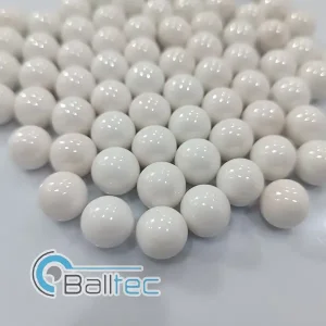
By leveraging nano-scale ceramic powder preparation using high-density Yttria-stabilized zirconia ($ZrO_2$) and high-purity alumina ($Al_2O_3$) milling media, manufacturers achieve exceptional dielectric constants ($\epsilon_r > 3000$) with uniform grain boundary structures.
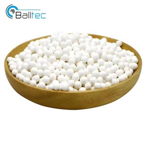
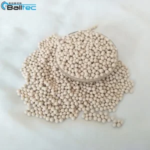
Humidity is the primary catalyst for dielectric breakdown and silver migration in ceramic capacitors. Utilizing 3A and 4A synthetic zeolite molecular sieve adsorbents during manufacturing packaging guarantees an ultra-dry ambient enclosure (< 1 PPM moisture level).
How integrated industrial clusters in Jiangxi and ceramic manufacturing hubs deliver unparalleled cost efficiency, scalable throughput, and rigorous quality control.
Global original equipment manufacturers (OEMs), component distributors, and tier-1 automotive suppliers increasingly source wholesale MOSFET capacitors, dielectric substrate powders, and specialized ceramic components directly from China. This procurement preference is driven by structural competitive advantages that extend far beyond raw unit cost savings.
China's industrial ceramic and electronic component hubs—exemplified by established clusters such as Pingxiang in Jiangxi Province—integrate raw material synthesis, precision powder atomization, calcination, iso-static pressing, high-temperature sintering, and automated optical inspection (AOI) within unified industrial zones. This proximity minimizes logistics overhead and accelerates production lead times from months to days.
Producing ceramic capacitors and high-density oxide balls requires continuous tunnel kilns and high-pressure sintering atmospheres operating consistently above $1600^\circ\text{C}$. Chinese manufacturing facilities leverage massive economies of scale, maintaining multi-gigawatt power grids, fully automated continuous ball-milling lines, and multi-tier quality control protocols under ISO 9001, ISO 14001, and ISO 45001 management frameworks.
| Material Category | Primary Chemical Composition | Dielectric / Mechanical Metric | Thermal Breakdown Limit | Key Application Scenario |
|---|---|---|---|---|
| High-Purity Alumina (99.99%) | $\alpha\text{-Al}_2\text{O}_3 \ge 99.99\%$ | Dielectric Strength: $30\text{ kV/mm}$ | $1750^\circ\text{C}$ | Substrate insulation, ultra-pure fine milling, high-voltage ceramic vacuum interrupters. |
| Yttria-Stabilized Zirconia (YSZ) | $\text{ZrO}_2 + 3\text{mol}\%\text{ Y}_2\text{O}_3$ | Density: $\ge 6.0\text{ g/cm}^3$, Toughness: $8-10\text{ MPa}\cdot\text{m}^{1/2}$ | $1450^\circ\text{C}$ | Nano-powder bead milling for MLCC dielectrics, wear-resistant high-speed bearing components. |
| 3A / 4A Synthetic Zeolite | $\text{K}_9\text{Na}_3[(\text{AlO}_2)_{12}(\text{SiO}_2)_{12}]\cdot x\text{H}_2\text{O}$ | Pore Size: $3\text{Å} / 4\text{Å}$, Water Adsorption: $\ge 21\%$ | Regeneration: $200-300^\circ\text{C}$ | Deep drying of electronic purge gases, semiconductor packaging moisture scavenging. |
| Zirconium Silicate Beads | $\text{ZrSiO}_4 \approx 65\%$ | Bulk Density: $4.0\text{ g/cm}^3$, Mohs Hardness: $7.5$ | $1200^\circ\text{C}$ | Cost-effective wet dispersion of non-metallic minerals, electronic pastes, and glaze milling. |
Custom engineering solutions tailored for high-reliability sectors across North America, Europe, East Asia, and emerging industrial markets.
On-Board Chargers (OBCs) and main traction inverters utilize SiC MOSFET switches operating at 800V DC architectures. Ceramic capacitors sourced for snubber protection require AEC-Q200 qualification, zero micro-cracking, and maximum surge current handling capabilities.
Hyperscale server power distribution units (PDUs) step down 48V bus bars to sub-1V point-of-load (POL) CPU/GPU cores using high-frequency multiphase Buck converter MOSFETs. High-k MLCCs provide instant transient current response during workload spikes.
Utility-scale battery energy storage system inverters employ robust MOSFET networks. The surrounding capacitive filter banks demand moisture-resistant dielectric encapsulation achieved through specialized 3A/4A zeolite desiccant purge atmospheres.
As semiconductor node sizes shrink and power densities surge, global procurement teams must balance three critical parameters when evaluating wholesale MOSFET capacitor factories:
In-depth technical answers addressing dielectric material selection, MOSFET gate drive optimization, and factory ordering procedures.
Explore our full line of high-density zirconia grinding balls, alumina ceramic spheres, and catalyst support media engineered for extreme duty cycles.