Follow 


Engineered ceramic components, high-purity alumina media, and structural packing elements supporting advanced electronic ceramic synthesis and industrial circuit processing.

Delivering zero-defect PCB manufacturing, advanced ceramic substrate synthesis, and continuous quality assurance for mission-critical electronic applications.
The global integrated circuit board (IC Board) industry is undergoing a structural paradigm shift driven by artificial intelligence (AI), 5G/6G wireless communication networks, electric vehicle (EV) powertrains, and high-performance computing (HPC) architectures. Traditional FR-4 organic laminates are increasingly encountering physical limits regarding dielectric loss ($D_f$), thermal dissipation, and structural mechanical rigidity. Consequently, advanced PCB design is rapidly adopting High-Density Interconnect (HDI), Substrate-Like PCB (SLP), and ceramic substrate technologies (Direct Bonded Copper - DBC, Active Metal Brazing - AMB) to satisfy aggressive miniaturization and power density demands.
Next-gen IC boards require signal transmission integrity at frequencies exceeding 28 GHz and 60 GHz. Utilizing PTFE, Hydrocarbon, and modified Polyimide resins reduces signal attenuation and phase distortion in RF modules.
With Wide Bandgap (WBG) semiconductors like Silicon Carbide (SiC) and Gallium Nitride (GaN) reaching thermal fluxes over 300 W/cm², ceramic substrates ($Al_2O_3$, $AlN$, $Si_3N_4$) provide unmatched thermal conductivity and matching Coefficient of Thermal Expansion (CTE).
Advancements in UV laser drilling enable blind and buried microvias with diameters under 50 µm. Anylayer HDI stackups allow direct vertical interconnectivity across multi-layer boards, dramatically increasing routing density for mobile and wearable devices.
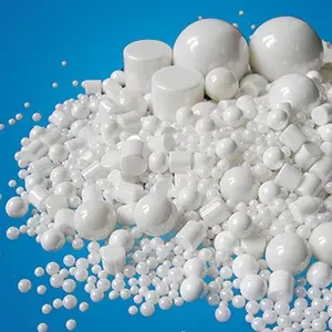
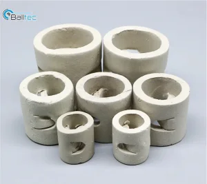
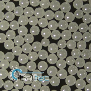
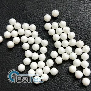
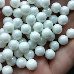
Technical Insight: Ceramic materials play a dual role in modern electronics. Beyond serving as rigid, thermally conductive circuit substrates (LTCC/HTCC/AMB), high-purity ceramic powders—refined via ultra-fine grinding media such as Yttria-Stabilized Zirconia (YSZ) beads—form the critical precursor materials for dielectric layers, passive chip components (MLCCs), and semiconductor package encapsulation.
Selecting the optimal substrate medium requires balancing electrical insulation, dielectric constant ($D_k$), dissipation factor ($D_f$), thermal performance, and mechanical strength. Below is a comparative technical synthesis across core industry substrate materials:
| Substrate Material | Thermal Conductivity (W/m·K) | Dielectric Constant (Dk @ 1GHz) | CTE (ppm/K) | Bending Strength (MPa) | Primary Application Areas |
|---|---|---|---|---|---|
| High-Tg FR-4 | 0.3 – 0.5 | 4.2 – 4.5 | 14 – 17 | 350 – 450 | Consumer Electronics, Industrial Control |
| High-Freq PTFE / Hydrocarbon | 0.5 – 1.0 | 2.2 – 3.0 | 10 – 12 | 200 – 300 | 5G Transceivers, Automotive Radar (77GHz) |
| Alumina ($Al_2O_3$ 96%) | 24 – 28 | 9.6 | 6.8 | 300 – 400 | LED Substrates, Automotive Sensor Modules |
| Aluminum Nitride (AlN) | 170 – 200 | 8.8 | 4.5 | 300 – 350 | High-Power Inverters, Laser Diodes, RF Amplifiers |
| Silicon Nitride ($Si_3N_4$) | 80 – 90 | 7.8 | 3.0 | > 700 | EV Powertrain Traction Inverters (AMB Technology) |
Sourcing integrated circuit boards and advanced ceramic substrates on an enterprise scale requires strict compliance with international manufacturing guidelines, design for manufacturing (DFM) verification, and robust risk-mitigated global supply chains. Corporate procurement teams at major Tier-1 automotive and aerospace firms evaluate suppliers across four critical vectors:
For high-reliability electronics, adherence to IPC-6012 Class 3 / 3A (Medical, Aerospace) and IATF 16949 (Automotive) is mandatory. This ensures continuous operational capability under severe environmental stress, zero annular ring breakout, and flawless microvia plating integrity.
Substrate performance depends entirely on raw material homogeneity. Supplier quality control extends to dielectric powder milling (ensuring trace impurities < 50 ppm using high-purity $ZrO_2$ or $Al_2O_3$ media), glass transition temp stability ($T_g$), and lot-level chemical batch certification.
Leading IC board factories utilize 100% Automated Optical Inspection (AOI) for inner/outer layer registration, Automated X-Ray Inspection (AXI) for multi-layer microvia alignment, Flying Probe testing, and Time-Domain Reflectometry (TDR) impedance validation (+/- 5% tolerance).
To avoid costly re-spins and engineering change orders (ECOs), procurement engineering teams must confirm supplier capabilities against explicit DFM parameters:
Challenge: Severe thermal cycling (-40°C to +175°C), high operational vibration, and high current densities in 800V EV powertrains breakdown standard organic substrates.
Solution: Implementation of Silicon Nitride Active Metal Brazing ($Si_3N_4$-AMB) ceramic substrate circuit boards. $Si_3N_4$ offers exceptionally high flexural strength (> 700 MPa) and fracture toughness, allowing direct soldering of SiC MOSFET dies with minimal thermal resistance.
Challenge: Processing power demand requires backplane IC boards with 32 to 64 layers, strict impedance match, and sub-100 fs timing jitter across ultra-fast PCIe 6.0 / 7.0 channels.
Solution: Ultra-low Df polyphenylene ether (PPE) laminates combined with smooth low-profile copper foil ($R_a < 1.0 \mu m$) to reduce skin-effect losses. Anylayer HDI microvias enable dense inter-layer routing between GPU accelerators and high-bandwidth memory (HBM) modules.
Challenge: High ambient atmospheric heat combined with millimeter-wave (mmWave) frequency transmission causing phase delays and localized thermal hotspots.
Solution: Hybrid stackup architecture pairing PTFE high-frequency layers on top of high-density Alumina ($Al_2O_3$) ceramic backings or heavy copper cores (up to 6 oz copper), enabling passive radiative thermal relief directly through the ground plane.
Operating a global supply chain demands seamless alignment with international environmental regulations, export compliance controls, and localized customer technical engineering support. Qualified integrated circuit board suppliers provide full transparency across product lifecycles:
All circuit boards and technical ceramic media conform strictly to RoHS 3 (EU Directive 2015/863), REACH (SVHC candidate list), and UL 94V-0 flammability ratings. Halogen-free laminates are available to support eco-friendly consumer electronics initiatives.
Suppliers mandate 100% Conflict-Free Smelters for 3TG minerals (Tantalum, Tin, Tungsten, Gold). Full CMRT (Conflict Minerals Reporting Template) documentation is rendered for seamless enterprise SEC compliance audit trails.
To reduce shipping lead times and support just-in-time (JIT) manufacturing line replenishment, localized distribution centers provide vendor-managed inventory (VMI), quick-turn prototype evaluation (< 48 hours DFM response), and regional engineering field support.
Strategic projection of substrate manufacturing technologies, interposer capabilities, and next-generation microelectronics packaging.
Transition from organic interposers to ultra-flat glass substrates offering high dimensional stability, zero warpage, and ultra-dense line/space geometries below 10 µm for next-gen chiplet packaging.
Integration of optical waveguides directly inside IC board substrates. Hybrid electro-optical printed circuit boards (EOPCB) eliminating copper trace loss for terabit-per-second server interconnects.
Development of ultra-pure ceramic and superconducting circuit boards optimized for cryogenic operating temperatures (< 4 Kelvin), minimizing thermal noise and quantum decoherence in quantum computers.
Ceramic substrates (such as Alumina $Al_2O_3$, Aluminum Nitride AlN, and Silicon Nitride $Si_3N_4$) provide vastly superior thermal conductivity compared to FR-4 (up to 170-200 W/m·K for AlN vs 0.3 W/m·K for FR-4). Additionally, ceramic boards possess a Coefficient of Thermal Expansion (CTE) ranging from 3.0 to 6.8 ppm/K, closely matching bare semiconductor silicon dies (3.5 ppm/K). This eliminates thermal expansion mismatch stress, dramatically reducing solder joint fatigue in high-power applications.
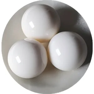
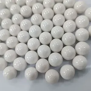
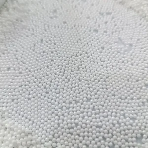
Advanced ceramic substrates and dielectric layers in MLCCs require sub-micron ceramic powders with tight particle size distributions and zero metallic contamination. Ultra-high density Yttria-Stabilized Zirconia (YSZ) grinding beads allow nano-milling of ceramic slurries down to sub-100 nm levels without introducing wear contamination, ensuring maximum dielectric breakdown voltage and mechanical strength in the finished board.
Direct Bonded Copper (DBC) bonds copper foil directly to alumina ($Al_2O_3$) at high eutectic temperatures (~1065°C). Active Metal Brazing (AMB) utilizes a brazing alloy containing active elements (like Titanium) to bond thick copper layers to Silicon Nitride ($Si_3N_4$) or AlN. AMB on $Si_3N_4$ yields significantly higher mechanical strength (> 700 MPa flexural strength) and thermal shock reliability, making it the preferred choice for automotive SiC EV traction inverters.
IPC-6012 Class 3 (and IPC-6012DS for automotive dedicated extensions) governs high-reliability rigid printed boards. Class 3 requires continuous inspection compliance, zero microvia plating voids, stricter drill registration tolerances, and guaranteed operational performance in continuous demanding environments such as automotive under-hood or aerospace flight control.
Microvia aspect ratio is the ratio of dielectric depth to laser-drilled hole diameter. The standard target ratio for reliable electroplating is 1:1 or 0.8:1 (e.g., a 75 µm deep via with a 75 µm diameter). Exceeding a 1.2:1 aspect ratio impedes liquid plating solution flow inside the via, increasing the risk of dimples, voids, and eventual open-circuit failures under thermal cycling.
Standard quick-turn prototypes for multi-layer HDI or ceramic circuit boards typically range from 5 to 9 working days following DFM approval. Mass production lead times generally range from 2 to 4 weeks depending on raw laminate availability, layer count, surface finish complexity (e.g., ENEPIG), and specialized testing requirements such as thermal stress baking or TDR impedance certification.
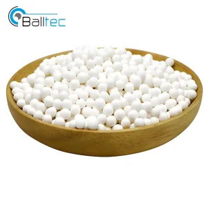
Advanced wear-resistant zirconia media, high-crush strength inert alumina support spheres, and low-impurity grinding solutions for sub-micron electronic material processing.