Follow 


High-purity ceramic solutions engineered to meet rigorous cleanroom and chemical planarization demands in modern transistor and diode fabrication pipelines.
Navigating the supply chain requirements for discrete semiconductor devices, power transistors, and advanced micro-component milling.
The international trade in discrete components—including Schottky diodes, MOSFETs, IGBTs, and bipolar junction transistors (BJTs)—demands zero defect tolerances. Global exporters must maintain consistent quality control from raw material synthesis to packaged component delivery, backed by reliable upstream material partners.
Next-generation power transistors fabricated on Silicon Carbide (SiC) and Gallium Nitride (GaN) substrates operate under extreme voltages and temperatures. Manufacturing these high-performance semiconductors requires sub-micron chemical-mechanical planarization (CMP) slurries milled with ultra-pure zirconia and alumina media.
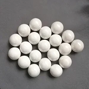
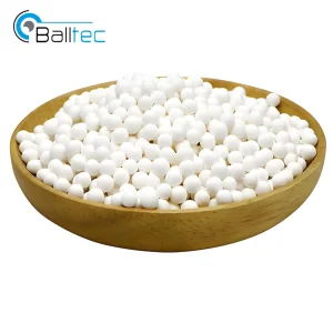
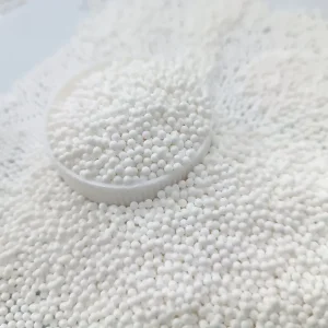
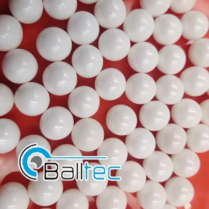
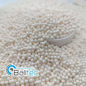
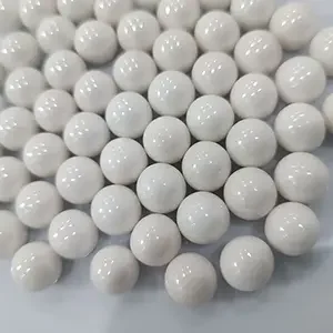
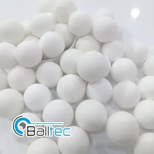
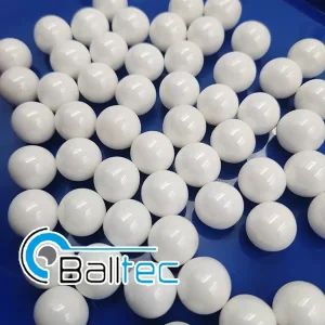
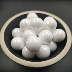
In discrete semiconductor production, trace elemental impurities (Fe, Na, Ca) can destroy PN junction characteristics and cause leakage currents. B2B exporters prioritize ultra-low wear media (such as 99.99% high-purity alumina and Y-TZP zirconia beads) to ensure zero metallic cross-contamination during ceramic substrate wet milling.
From ultra-pure gas dehydration to sub-micron slurry dispersion, industrial ceramic solutions form the operational foundation for semiconductor manufacturing.
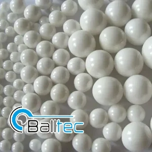
Chemical-Mechanical Planarization (CMP) is vital for achieving atomic-level flatness on semiconductor wafers before gate formation. High-density Yttria-Stabilized Zirconia (YSZ) beads allow high-energy micro-milling of silica, ceria, and alumina abrasive particles to sub-100nm size distributions without introducing lattice-disrupting contaminants.
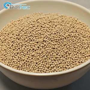
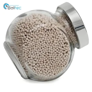
Synthetic gas streams used in chemical vapor deposition (CVD) and epitaxy for transistor fabrication require moisture levels below parts-per-billion (ppb). 3A, 4A, and 5A Zeolite Molecular Sieves dynamically adsorb trace moisture, methanol, and volatile impurities from carrier gases like Nitrogen, Argon, and Hydrogen.
High-speed pick-and-place equipment and vacuum transfer arms used in diode testing lines utilize G3 and G5 precision Silicon Nitride (Si3N4) and Zirconia ceramic bearing balls. These components offer complete electrical insulation, non-magnetic operation, and maintenance-free service under vacuum environments.
| Material Property | Y-TZP Zirconia Beads (6.0 g/cm³) | High Purity Alumina 99.99% | Standard Ceramic Balls |
|---|---|---|---|
| Density (g/cm³) | > 6.00 | 3.85 - 3.95 | 2.40 - 2.70 |
| Vickers Hardness (HV10) | 1,250 - 1,350 | 1,600 - 1,750 | 650 - 800 |
| Impurity Level (ppm) | < 50 ppm (Ultra-Low) | < 100 ppm | > 1,500 ppm |
| Wear Rate (ppm/hr) | < 0.005% | < 0.015% | > 0.15% |
| Primary Application | Semiconductor Slurry / Battery Nano Milling | Electronic Substrates / Bio-Inert Components | General Industrial Milling |
Supporting component exporters, semiconductor foundries, and packaging facilities in key industrial regions worldwide.
Exporters of automotive-grade IGBT modules and fast-recovery diodes for Electric Vehicle inverters rely on ceramic substrates milled with ultra-pure zirconia to maximize thermal conductivity and prevent dielectric breakdown during high-voltage switching.
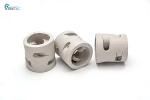
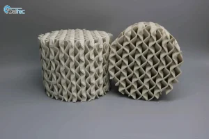
High-efficiency solar photovoltaic systems require robust bypass diodes and silicon carbide MOSFETs. Production of these components involves precise chemical scrubbing towers packed with high-efficiency ceramic corrugated plate packings to handle corrosive acid etching vapors.
RF GaN-on-SiC transistors operating at millimeter-wave frequencies require zero surface defects. Nano-polishing powders dispersed using ultra-fine ZrO2 beads guarantee clean wafer surfaces, ensuring low noise figures and high amplification efficiency.
Providing full traceability, international standard compliance, and localized engineering support to simplify B2B procurement.
All advanced ceramic materials and molecular sieves adhere strictly to ISO 9001 quality management, ISO 14001 environmental safety, REACH regulations, RoHS directive restrictions, and Conflict Mineral Compliance guidelines.
Every shipment is backed by comprehensive Certificate of Analysis (CoA) testing, X-Ray Fluorescence (XRF) purity analysis, and laser diffraction particle size distribution (PSD) reports to ensure lot-to-lot consistency.
We provide custom micro-bead sizing (down to 0.05mm), tailormade molecular sieve mesh sizes (1.6-2.5mm, 3-5mm), and specialized cleanroom-compatible double vacuum sealed export packaging for sensitive cleanroom destinations.
Strategic development paths targeting next-generation semiconductor, energy storage, and microelectronics requirements.
Commercialization of ultra-small 0.03mm Y-TZP beads for next-gen CMP slurries used in 2nm logic gate and advanced transistor node planarization.
Development of microcrystalline AlN and high-purity zirconia formulations designed for direct substrate mounting in high-power diode packages.
Integration of fully automated, AI-monitored sintering processes powered by green hydrogen to deliver carbon-neutral advanced ceramics for worldwide export.
Detailed technical answers to common queries regarding advanced materials, export logistics, and semiconductor processing applications.
Explore our specialized chemical packings, high-purity alumina media, molecular sieves, and precision ceramic balls available for international bulk export.