Follow 


Factory-direct high-density media, ceramic substrates, and advanced process components engineered for ultra-fine circuit fabrication and electronic manufacturing.


Modern electronics require wholesale electronic PCB manufacturers to bridge ultra-fine line pitch engineering, ceramic material integration, and high-frequency signal integrity.
As semiconductor nodes shrink below 3nm, board-level interconnect density must evolve synchronously. High-Density Interconnect (HDI) structures utilizing modified Semi-Additive Processes (mSAP) allow line width and spacing (L/S) to scale down to 15µm/15µm. Through laser direct imaging (LDI) and chemical micro-etching, our production protocols eliminate traditional mechanical routing tolerance stack-ups.
Stacked microvias filled with electroplated copper enable seamless signal transit across 10+ layer stack-ups. This structural density is imperative for AI accelerators, edge compute units, and miniaturized IoT devices where board real estate commands a massive premium.
5G millimeter-wave (mmWave) networks and automotive radar arrays operating at 77GHz require dielectric materials with ultralow loss tangents ($Tan\,\delta < 0.0015$). We specialize in hybrid stack-ups incorporating Rogers RO4350B, Taconic, PTFE, and ceramic-filled hydrocarbon laminates bonded to traditional FR-4 cores.
For high-power electronics—such as EV power inverters and RF base stations—we integrate Direct Bonded Copper (DBC) and Active Metal Brazing (AMB) ceramic substrates (Al2O3, AlN, Si3N4). These inorganic layers yield thermal conductivities ranging from 24 W/mK to over 180 W/mK, eliminating thermal throttling in mission-critical applications.
| Substrate Classification | Dielectric Constant ($D_k$ @ 10GHz) | Dissipation Factor ($D_f$ @ 10GHz) | Thermal Conductivity | Target High-Tech Application |
|---|---|---|---|---|
| High-TG FR-4 (Isola 370HR) | 4.17 | 0.0161 | 0.4 - 0.5 W/mK | Industrial Automation, Computing Backplanes |
| Hydrocarbon / Ceramic (Rogers 4350B) | 3.48 | 0.0037 | 0.69 W/mK | 5G Infrastructure, Automotive Radar |
| PTFE Glass-Reinforced (Taconic TLX) | 2.45 | 0.0019 | 0.45 W/mK | Satellite Communications, Aerospace Systems |
| Alumina Ceramic Substrate ($Al_2O_3$) | 9.80 | 0.0003 | 24 - 30 W/mK | LED Modules, Automotive Sensors |
| Silicon Nitride AMB Ceramic ($Si_3N_4$) | 8.30 | 0.0005 | 90 - 180 W/mK | EV Traction Inverters, Aerospace Power Modules |
Anticipating next-generation hardware requirements: From 800G optical transceivers to embedded chiplet packaging systems.
The convergence of IC substrate technologies and traditional printed circuit boards is driving wholesale electronic PCB manufacturers toward sub-10µm geometry fabrication. By adopting advanced SAP chemistries, ultra-thin seed copper layers, and semi-additive pulse electroplating, our facilities achieve crisp trace profiles with structural aspect ratios exceeding 1.5:1.
Hyperscale datacenters demands transition from copper interconnects to optical pathways at the board level. Our thermal engineering roadmap integrates embedded glass waveguides and precision-etched optical cavities directly within multi-layer rigid-flex boards, mitigating signal degradation in 800G and 1.6T networking hardware.
To eliminate parasitic inductance caused by SMT solder joints, modern PCB architectures embed passive components (capacitors, resistors) and active silicon dice into inner core cavities. Controlled laser ablation, resin filling, and micro-via plating yield fully planar surface topologies for ultra-dense wearable and military electronics.
Tailor-engineered PCB architectures customized for high-reliability, zero-defect operating environments across global industries.
Electric powertrains demand heavy copper PCBs (up to 12oz) combined with ceramic AMB substrates capable of handling 800V DC-DC converters and high-surge battery management systems (BMS). Our automotive manufacturing lines implement strict statistical process control (SPC), thermal cycle stress testing (-40°C to +175°C), and 100% ionic contamination testing.
IPC-6012 Class 3 / 3A compliant circuit fabrications engineered for harsh environments subject to high vibration and G-force shocks. Utilizing polyimide high-TG materials, sequential lamination (Seq-Lam), and thick gold plating (ENEPIG), our defense-grade circuit boards ensure zero field failure rates in flight controls, radar, and satellite transponders.
Ultra-flexible, biocompatible rigid-flex PCBs designed for medical implants, endoscopic imaging probes, and diagnostic telemetry systems. Features micro-scale surface mount technology (SMT 01005 / 008004 pitch), precision laser-excised flex tails, and hydrophobic conformal coatings for fluid-resistant longevity.
Leveraging fully integrated smart factory infrastructure to guarantee raw material buffering, automated yield optimization, and rapid global distribution.
Our 100,000 m² smart manufacturing campus integrates real-time Manufacturing Execution Systems (MES) and IoT-driven equipment monitoring. From raw laminate automated storage and retrieval systems (ASRS) to fully automated chemical plating lines, digital twin technology tracks every production panel through 120 distinct processing checkpoints.
Automated Optical Inspection (AOI) powered by machine learning algorithms evaluates outer-layer etching down to sub-pixel anomalies, reducing human inspection error to absolute zero. Closed-loop chemical dosing maintains bath concentration within ±1.5% margins, guaranteeing consistent copper grain structure across millions of square feet annually.
Supply chain volatility can jeopardize project timelines. As an integrated manufacturer, we maintain strategic reserves of high-purity ceramic substrates ($Al_2O_3$, $Zr_O2$, $AlN$), electro-deposited copper foils, and specialty resin systems directly within our regional industrial hubs.
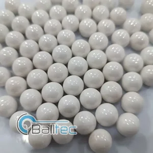
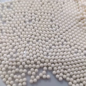
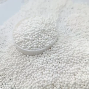
By coupling core PCB fabrication with specialized micro-machining, ceramic ball milling, and precision surface treatment under one umbrella, we eliminate third-party subcontractor lead times. This vertical synergy lowers Total Cost of Ownership (TCO) by up to 22% while providing 10-day standard turnarounds on complex multi-layer production runs.
Systematic engineering support from NPI (New Product Introduction) prototype stages to high-volume commercial scaling.
Every Gerber, ODB++, or IPC-2581 dataset undergoes a rigorous 32-point DFM check by our senior CAM engineers. We evaluate aspect ratios, copper balance, annular ring clearance, impedance track profiles, and solder mask expansion to eliminate production bottlenecks before physical laminates are loaded.
Accelerate time-to-market with our rapid NPI prototyping cells. We validate stack-up geometries, test micro-via reliability, and provide TDR impedance measurement reports. Once validated, production profiles transition automatically to automated high-volume lines without requiring re-qualification.
End-to-end EMS services including component sourcing (franchised distribution networks), high-speed SMT placement (008004 components), 3D SPI (Solder Paste Inspection), 3D X-ray inspection for BGA/QFN voiding, functional testing, and full electro-mechanical box build integration.
Strict international standard compliance ensures frictionless import, environment-friendly manufacturing, and seamless global logistics.
Our global operations strictly adhere to international environmental and quality benchmarks. Production lines hold ISO 9001, ISO 14001, ISO 45001, IATF 16949, and ISO 13485 certifications. All raw materials comply with UL 94V-0 flammability ratings and IPC-6012/6013 quality standards.
We are fully committed to sustainable manufacturing processes. All surface finishes—including Lead-Free HASL, ENIG, ENEPIG, and Immersion Silver—are 100% compliant with EU RoHS 3.0 and REACH SVHC directives. Wastewater processing systems recycle 85% of industrial process water.
Operating dedicated logistics nodes across North America, Europe, and Asia-Pacific, we offer tailored logistics options ranging from Express Air Freight (DHL/FedEx) to DDP (Delivered Duty Paid) sea and rail freight. Custom vacuum-sealed ESD packaging guarantees pristine shelf life upon arrival.
Expert insights addressing complex procurement, engineering, and material selection questions.
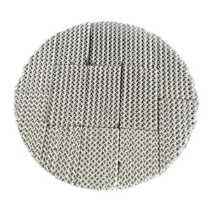
Explore our complete high-performance catalog engineered for heavy industrial ball milling, ceramic packing towers, and high-purity powder refinement.