Follow 


Engineered for extreme wear resistance, ultra-low dielectric dissipation, and chemically inert surface purity required across semiconductor, battery slurry, and electronic component manufacturing.
In modern microelectronics, high-frequency telecommunications, and high-power density conversion, traditional metallic and polymer-based materials face distinct limits in breakdown voltage, mechanical fatigue, and thermal conductance.
High-frequency electronics operating in millimeter-wave bands (5G/6G sub-THz regimes) require dielectric substrates with exceptional dimensional stability and microstructural uniformity. Advanced ceramic formulations, specifically ultra-pure 99.99% Al2O3 and stabilized tetragonal zirconia, provide loss tangents down to 10⁻⁴, preventing signal attenuation and inter-trace crosstalk across multi-chip modules (MCM).
Power semiconductors (SiC MOSFETs, GaN HEMTs) generate localized heat fluxes exceeding 500 W/cm². Ceramic structural elements and fine-grained substrates serve as direct-bonded copper (DBC) or active metal brazed (AMB) backbones. Their thermal expansion coefficients (CTE) tightly align with silicon and wide-bandgap dies, eliminating mechanical delamination under thermal cycling from -55°C to 175°C.
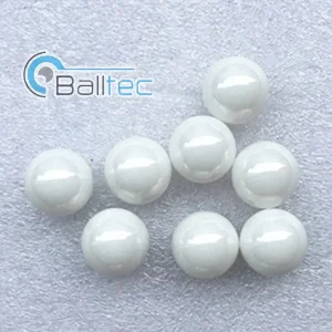
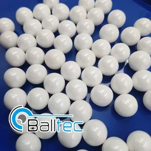
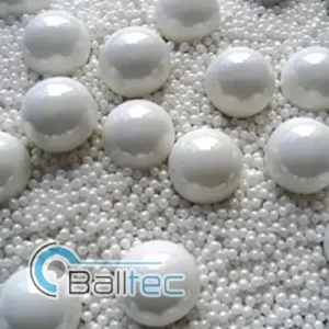
Electronic passive components, including Multilayer Ceramic Capacitors (MLCC) and low-temperature co-fired ceramics (LTCC), demand raw precursor powders ground to d50 < 50nm without metallic contamination. Utilizing Y-TZP (Yttria-Stabilized Tetragonal Zirconia Polycrystal) grinding media guarantees near-zero contamination wear (< 0.5 ppm/hour), ensuring reproducible dielectric breakdown voltages.
Translating basic physical-chemical properties into repeatable production solutions for automotive, industrial robotics, clean energy, and analytical systems.
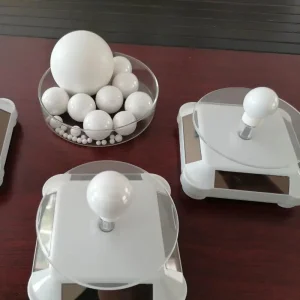
Electric vehicle e-axles and high-rpm motors operate under severe electrical fields where stray capacitive currents generate electrical erosion in steel bearings. Hybrid bearings incorporating G3/G5 precision zirconia (ZrO2) and silicon nitride (Si3N4) balls break galvanic loops, prevent pitting, and allow rotational velocities beyond 22,000 RPM in transmission oil environments.
Semiconductor vacuum chambers rely on ceramic guide rings and bearing components that eliminate the need for organic hydrocarbon lubrication. Ceramic elements resist outgassing in ultra-high vacuum (UHV) conditions (< 10⁻⁸ Torr) while maintaining dimensional stability across wide temperature profiles inside chemical vapor deposition (CVD) equipment.
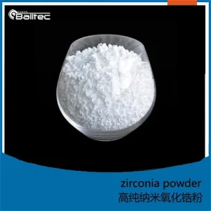
Through closely regulated yttrium doping levels (3mol% to 8mol% Y-TZP), our ceramic powders provide targeted oxygen-ion conduction profiles for Solid Oxide Fuel Cell (SOFC) membranes and nascent solid-state electrolyte separators, achieving cubic/tetragonal phase stabilization under high-temperature sintering.
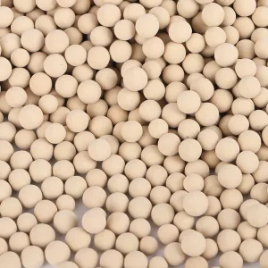
Electronic chemicals—including high-purity silane, phosphine, and semiconductor cleaning solvents—demand trace moisture removal below 1 ppm. Our Type 3A, 4A, and 13X synthetic zeolite molecular sieves possess tightly controlled window apertures, ensuring deep dehydration and amine/methanol scrubbing without catalytic degradation.
Operating from the historic ceramic cluster in Pingxiang, Jiangxi, our 100,000-square-meter campus combines automated raw material dosing, cold isostatic pressing (CIP), precision continuous tunnel kilns, and laser sphericity inspection to produce over 25,000 metric tons annually.
Tier-one OEMs in North America, Europe, and Asia-Pacific demand suppliers that integrate manufacturing scale with thorough quality compliance and export transparency.
Every shipment is accompanied by complete inspection data: Mill Test Certificates (MTC), Certificate of Analysis (CoA) via XRF/ICP-MS, and particle size distribution (PSD) laser graphs. Our manufacturing plants maintain ISO 9001:2015, ISO 14001:2015, and ISO 45001 certifications.
Our raw material chemistry is free of hazardous substances listed under EU RoHS Directive 2011/65/EU and REACH SVHC regulations. Raw minerals are sourced in strict adherence to OECD Due Diligence Guidance, ensuring transparent supply chains free from conflict materials.
Industrial ceramics and precision beads require careful packaging to avoid moisture ingress and transit attrition. We provide UN-certified steel drums, vacuum-sealed bags with desiccants, and fumigated timber pallets with shrink-wrap protection for global ocean and air freight.
Anticipating emerging requirements across advanced electronics, quantum hardware, and next-generation power distribution architectures.
Commercialization of Zirconia Toughened Alumina (ZTA) media featuring sub-100nm crystal grain size, enabling horizontal bead milling of conductive silver inks and carbon nanotube (CNT) suspensions with minimal energy input.
Advancing stereolithography (SLA) and binder-jetting techniques for ultra-pure alumina and zirconia slurries, enabling complex internal cooling microchannels for direct liquid-cooled power electronics packages.
Developing stabilized cubic garnet-type LLZO (Lithium Lanthanum Zirconium Oxide) and next-generation ceramic frameworks to enable 1000Wh/L solid-state battery cells for automotive and aerospace applications.
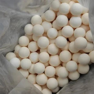
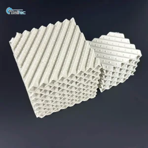
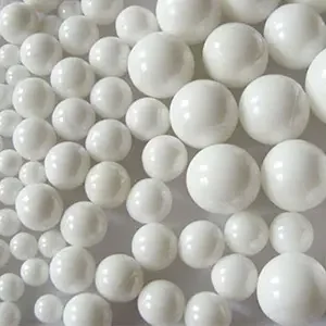
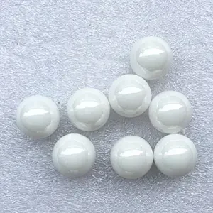
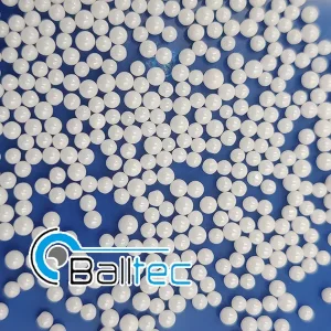
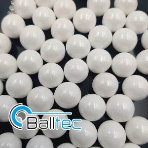
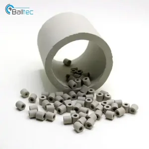
Discover our comprehensive range of high-density grinding beads, random column packings, and engineered ceramic powders for fine electronic powder processing.
Direct engineering responses addressing material composition, wear kinetics, and qualification pathways.