Follow 


Retaining core manufacturing precision across advanced ceramics, substrate powders, and specialized thermal elements engineered for semiconductor processing equipment and industrial applications.


Navigating Silicon (Si), Silicon Carbide (SiC), and Gallium Nitride (GaN) Technologies for Industrial, Automotive, and High-Density Power Systems.
From low-forward-voltage ($V_F$) Schottky Barrier Diodes (SBD) to ultra-fast recovery diodes (FRD) and Transient Voltage Suppressors (TVS), discrete diodes remain the cornerstone of power rectification, circuit protection, and signal demodulation.
Encompassing Small Signal BJTs, Field-Effect Transistors (MOSFETs), and Insulated-Gate Bipolar Transistors (IGBTs). Specialized for high-frequency switching, conduction-loss reduction, and high-current industrial motor drives.
3rd-generation semiconductors enabling elevated breakdown voltages ($>1200\text{V}$), reduced switching energy ($E_{off}$), and operating thermal limits exceeding $175^\circ\text{C}$ for electric vehicles and renewable energy storage.
Selecting the optimal semiconductor substrate requires analyzing thermal impedance, reverse recovery time, and breakdown voltages.
| Material Parameter / Property | Silicon (Si) Standard | Silicon Carbide (SiC) | Gallium Nitride (GaN) | Engineering Impact |
|---|---|---|---|---|
| Bandgap Energy (eV) | 1.1 eV | 3.26 eV | 3.4 eV | Higher bandgap drastically reduces intrinsic carrier generation at high temperatures. |
| Critical Breakdown Field (MV/cm) | 0.3 MV/cm | 2.8 MV/cm | 3.3 MV/cm | Allows thinner drift layers, yielding substantially lower On-State Resistance ($R_{DS(on)}$). |
| Thermal Conductivity (W/m·K) | 1.5 W/m·K | 4.9 W/m·K | 1.3 W/m·K | SiC excels in passive heat dissipation, drastically minimizing heatsink volumetric footprint. |
| Electron Mobility ($\text{cm}^2/\text{V}\cdot\text{s}$) | 1400 | 900 | 2000 | GaN enables ultra-high frequency switching ($> 1\text{ MHz}$) for lightweight power supplies. |
| Reverse Recovery Charge ($Q_{rr}$) | Moderate to High | Near Zero (Schottky) | Zero (No Body Diode) | Eliminates primary switching turn-on losses in totem-pole PFC topologies. |
While SiC MOSFETs and GaN HEMTs carry a higher unit ASP (Average Selling Price) compared to legacy Silicon MOSFETs, their elevated switching speed permits up to a 60% reduction in magnetic component size (inductors, transformers) and filter capacitors, delivering a net reduction in overall System Level BOM Cost.
Leveraging vertically integrated OSAT (Outsourced Semiconductor Assembly and Test) hubs in Guangdong, Jiangsu, and Zhejiang to provide unmatched cost-to-performance scale.
State-of-the-art automatic lead-frame bonding, clip-bonding technology (Copper Clip), and transfer molding for SOT-23, TO-252 (DPAK), TO-263 (D2PAK), DFN, and TO-247 packages, ensuring low thermal resistance ($R_{th(j-c)}$) and ultra-low parasitic inductance.
Our manufacturing partners adhere strictly to zero-defect quality management framework. Every automotive-certified diode and MOSFET undergoes 100% Automated Optical Inspection (AOI), Parametric Wafer Testing, and High-Temperature Reverse Bias (HTRB) testing.
Mitigate single-source geopolitical and supply risks. We offer direct pin-to-pin drop-in replacements for top global discrete brands (such as Vishay, Diodes Inc., ON Semi, Infineon, and Nexperia) with guaranteed lead times under 4–6 weeks.
How advanced diode and transistor innovations are accelerating key industrial growth sectors globally.
AEC-Q101 High-Voltage SiC Diodes and SiC MOSFETs used in On-Board Chargers (OBC), Main Traction Inverters, and DC-DC converters to maximize battery range and enable 800V fast-charging architectures.
1200V / 1700V IGBT modules and high-speed body diode MOSFETs used in Photovoltaic (PV) String Inverters and Utility-Scale Battery Energy Storage Systems (BESS) for high MPPT efficiency.
GaN HEMTs and Low-Rds(on) Synchronous Rectification (SR) MOSFETs tailored for 80 Plus Titanium Common Redundant Power Supplies (CRPS) serving AI GPU clusters and cloud servers.
Miniaturized DFN/CSP packaged Schottky Diodes and Load Switch MOSFETs deployed in high-density USB Type-C Power Delivery adapters, smartphones, wearables, and IoT edge devices.
Streamlining Component Selection, Quality Audit, Lifecycle Management, and Logistics Security.
We provide guaranteed minimum 10-year product longevity for industrial and automotive clients. Product Change Notifications (PCN) and End-of-Life (EOL) notices are issued at least 12 months in advance with Last-Time-Buy (LTB) support.
Every reel, tube, and tray features unique 2D Matrix Barcode tracking tied directly to wafer lot numbers, lead-frame batch numbers, and final test inspection data sheets for complete supply chain transparency.
To eliminate factory downtime during global semiconductor shortages, we provide Vendor-Managed Inventory (VMI) and regional consignment buffer stock options in key logistics hubs (Hong Kong, Shenzhen, Europe, US).
Addressing technical parameters, qualification standards, ESD protection, thermal management, and procurement workflows.
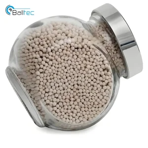
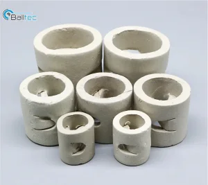
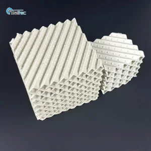
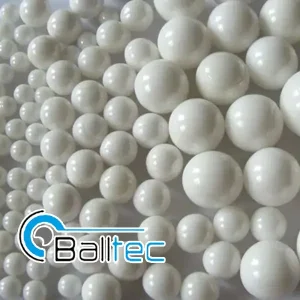
Retaining full cross-industry catalog availability, including high-purity milling media, tower packing, and ceramic precision components.
Looking for direct factory pricing, parametric cross-reference mapping, or custom wafer packaging solutions? Contact our senior engineering team today for response within 12 hours.
Submit Technical RFQ