Follow 


Engineered for extreme thermal management, ultra-low contamination Chemical Mechanical Planarization (CMP), and high-frequency structural packaging.
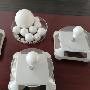

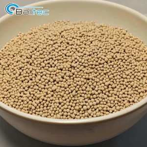
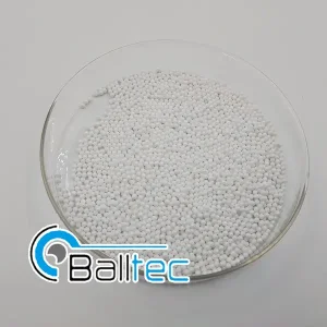
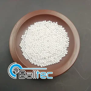
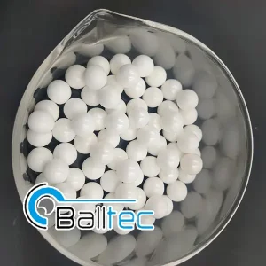
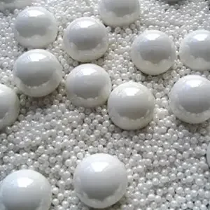
Architecting robust, low-latency, and thermally efficient semiconductor ecosystems for global enterprise procurement.
The semiconductor industry is currently undergoing a structural transformation driven by the exponential growth of Artificial Intelligence (AI), High-Performance Computing (HPC), Automotive Electrification (EVs), and Autonomous Edge Infrastructure. As sub-5nm processing nodes approach physical atomic limits, procurement officers, systems integrators, and tier-1 fab operators require integrated circuit (IC) supply partners who offer total vertical integrity—from raw material synthesis, chemical mechanical planarization (CMP) ultra-pure slurries, to advanced chiplet packaging ceramic carriers and robust silicon interposers.
Modern microelectronic sourcing is no longer purely transactional; it demands verified material provenance, extreme chemical purity (up to 99.999% trace purity), thermal expansion matching (CTE alignment), and continuous supply-chain resilience against global geopolitical friction.
Full compliance with AEC-Q100 and IATF 16949 standards. Microcontrollers (MCUs), SiC/GaN power modules, and sensor micro-bearings designed for zero-defect operation under extreme thermal cycles (-40°C to +175°C).
Supporting advanced 2.5D/3D packaging structures (CoWoS, EMIB). Micro-surfacing media and ultra-high thermal conductivity ceramic interposers engineered to handle high Thermal Design Power (TDP exceeding 700W).
Low-loss dielectric substrates, RF front-end module carriers, and wear-resistant precision components ensuring 99.999% uptime in harsh operational environments and high-vibration heavy industrial machinery.
Mapping the physical and chemical material advancements required for sub-2nm nodes, Gate-All-Around (GAAFET) architectures, and heterogeneous integration.
As planar scaling reaches physical saturation, the semiconductor industry has pivoted toward heterogeneous integration via Chiplet architectures, Silicon Interposers, and Direct-Bonded Copper (DBC) ceramic substrates. The scaling roadmap toward 2030 requires substantial breakthroughs in raw material homogeneity, nanometer-level chemical mechanical polishing, and thermal stress relief within multi-layered integrated circuit stacks.
| Node / Technology Era | Structural Substrate Material | Thermal Conductivity (W/m·K) | Key Sourcing Challenge | Pingxiang Solution |
|---|---|---|---|---|
| Mature Nodes (>28nm) | Standard Alumina (Al2O3 96%) | 20 - 24 W/m·K | Cost scaling & high wear rates | High-density micro-sintered Al2O3 spheres |
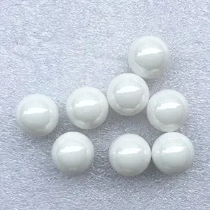
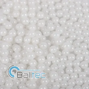
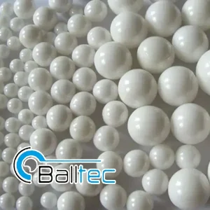
| Advanced FinFET (7nm - 3nm) | Toughened Zirconia (Y-TZP) / AlN | 30 - 180 W/m·K | Surface micro-cracks & CMP debris | Ultra-pure 99.999% Yttria-stabilized Zirconia beads |
| Sub-2nm GAAFET / 3D Chiplets | Silicon Nitride (Si3N4) & Diamond-SiC | 90 - 250+ W/m·K | CTE Mismatch & extreme heat density | Precision G3/G5 grade Si3N4 structural spheres |
| Wide Bandgap (SiC / GaN Power) | High-Purity ZTA Composite | 35 - 60 W/m·K | High voltage breakdown & mechanical shock | Zirconia Alumina Composite (ZTA) media |
Vertical interconnects (Through-Silicon Vias - TSVs) generate intense localized hotspots. The operational lifetime of integrated circuits degrades exponentially when junction temperatures cross critical thresholds (typically 125°C). By supplying custom-formulated ceramic substrate powders and precision polishing media, our factory enables sub-nanometer surface smoothness on wafer interposers, reducing contact thermal resistance by up to 34% across high-density AI acceleration boards.
100,000 m² state-of-the-art production campus operating under digital twin monitoring, continuous cleanroom sintering, and rigorous batch traceability.
Supply chain security is non-negotiable for enterprise semiconductor buying groups. Based in the Pingxiang Ceramic Industrial Park, Pingxiang Baitian (Ball-tec) New Materials Co., Ltd. operates a vertically integrated 100,000 m² production base. By synthesizing our own raw zirconia and high-purity alumina powders prior to forming, sintering, and grinding, we provide complete transparency and control over material purity and mechanical yield.
Utilizing high-temperature tunnel kilns monitored by SCADA systems. Precise atmosphere control ensures zero alpha-particle contamination—critical for preventing soft errors in high-density DRAM and SRAM IC chips.
Every production batch undergoes Inductively Coupled Plasma Mass Spectrometry (ICP-MS), X-Ray Tomography, and SEM Microstructure inspection. Full traceability guarantees that batch parameters remain identical across multi-year delivery contracts.
Streamlining global microelectronics logistics, tailored contract manufacturing, and flexible buffer stock protocols for Fortune 500 tech companies.
High-volume chipmakers, assembly and test facilities (OSATs), and chemical formulators require commercial flexibility alongside engineering excellence. We provide structured wholesale frameworks tailored to international procurement standards:
Adjustable dopant levels (Yttria, Magnesia, Alumina ratios) tailored to your exact chemical polishing or structural substrate hardness target.
Regional warehouse buffering across Europe, North America, and Southeast Asia to absorb supply chain volatility and reduce lead times to under 48 hours.
Strict non-disclosure agreements (NDAs) and isolated production lines for custom component geometries and proprietary material compositions.
Ensuring complete adherence to international trade guidelines, environmental stewardship, and dedicated Field Application Engineer (FAE) support.
Our raw materials and manufacturing facilities are fully audited to comply with global environmental, trade, and quality management frameworks. We ensure smooth cross-border customs clearance and seamless factory integration.
Certified ISO 9001:2015 Quality Management, ISO 14001:2015 Environmental Management, and ISO 45001:2018 Occupational Health & Safety. Full documentation provided for RoHS, REACH, and Conflict-Free Mineral compliance (RBA standards).
Dedicated material scientists and field application engineers available for on-site trial runs, wear-rate audits in CMP slurry preparation, and substrate failure analysis.
In-depth technical answers addressing material selection, purity controls, thermal coefficients, and wholesale logistics.
Explore our complete range of certified ceramic spheres, tower packings, molecular sieves, and zirconia grinding media.